This article is more than 1 year old
Why Flash storage will be fast and furious in 2014
We look in the rear view mirror before racing down the road ahead
Flash had a fantastic year in 2013 with an enormous number of developments.
It was a year of generally positive flash transitions, with cell geometry shrinking, all-flash arrays springing up, flash companies being bought, flash companies crashing back to earth after inflated IPOs or just crashing, and happiness spraying out like sunshine from three hybrid flash/disk array suppliers.
Trying to keep up with all this and fit it into a big picture was like trying to sip delicately from the water coming over Niagara Falls.
Still, some things became apparent from under the drowning flood of product and technology flash news. There began to be a general acceptance that access to I/O intensive random data was best done using flash rather than disk and that all-flash arrays definitely had a role as the best container for networked storage of hot, random data. Disk was as good as flash for streaming data and also much cheaper on a $/GB basis. So-so disk arrays were best for nearline, cool and possibly cold data, and also for large files with streaming access.

Flash all the way with the Jobs' Mob's Macbook Air
The consensus view was that fast thin and light notebooks needed flash for the best performance, as did tablets. But thin and hybrid 2.5-inch flash+disk drives could be used, manufacturers started suggesting, in both tablet and ultralite form factors to provide flash speed for hot data and cheaper disk capacity for the relatively bulk cool data.
We'll look at the business side of things in a later article, but right now let's take a look at developments in flash technology.
Not a lot of TLC
We didn't see triple-level cell (TLC) NAND push into enterprise applications in 2013, TLC flash being slow and having a ridiculously short write endurance level. Also flash foundries prefer to make single and multi-level cell (SLC and MLC) on their foundry production lines because these command higher volumes and deliver a better return on manufacturing investment. TLC flash remains relegated to thumb drives, camera flash cards and the like.
There was the beginning of a transition towards 1X (19nm-10nm) flash cell geometries from the 2X (29nm - 20nm) technology. Toshiba for example is building 19nm kit now. As a reminder the smaller the geometry the more NAND flash chips can be cut from a wafer, thus lowering the cost/GB. However the shift is not even across the industry; Micron is transitioning to 20nm now with a 16nm process starting production samples this year.
Building up to 3D NAND
One thing that didn’t happen was the emergence of any non-volatile technology to take over from flash. It’s generally agreed that flash technology may be unable to develop usable enterprise flash storage with acceptable endurance down at 15nm and below. Phase Change Memory and varieties of Resistive RAM, such as HP’s Memristor, are still future tech, with 3D NAND taking up the capacity slack by cramming more flash layers onto a flash chip with connecting tunnels (through Silicon Vias or TSVs) linking the layers to a base logic layer.
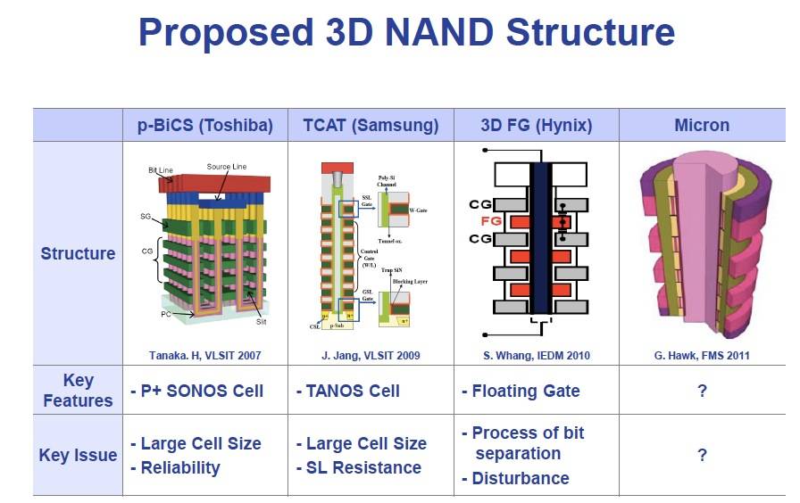
3D NAND schematic diagram. Click picture for larger version.
Micron expects to commence 3D NAND production sample shipments before mid-2014, perhaps as early as by April. But volume production won’t take place until 2015. Samsung heavily publicised its 3D_VNAND technology but production doesn’t actually look to start production this year and it’s not an orderable product.
Jim Handy of Objective analysis produced a fine series of 3D NAND papers on his Memory Guy web site, discussing the technology and manufacturers’ plans.
