This article is more than 1 year old
SanDisk shows off multi-level cell make-over
X4 and X3 flash dies
SanDisk and Toshiba have announced the world's smallest NAND flash die and the world's highest-capacity flash die using 32nm and 43nm process technologies.
At the International Solid State CIrcuits Conference in San Francisco the two announced they will start manufacturing the world's highest-capacity 64Gbit die using 4-bits-per-cell (X4) multi-level cell (MLC) technology. By packing more bits into a single flash cell the capacity of the cell and the die (chip) is part of the increases. This die uses 43nm process technology and was co-developed by Toshiba and SanDisk. The X4 controller needed to manage the reading and writing of data to/from it was developed by SanDisk alone. A multi-chip package combining controller and die will be available from SanDisk.
Its performance is 7.8MB/sec when writing data which is said by SanDisk to be comparable with current MLC, meaning X3 ones we think. SanDisk announced its X3 MLC technology at last year's ISSCC event.
An issue in the abortive attempt by Samsung to take over SanDisk last year was SanDisk wishing to charge more for licensees like Samsung to use the then coming X4 technology.
32nm X3 die
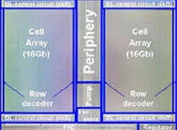
Toshiba and SanDisk also announced the world's smallest microSD NAND flash die, 113 square millimetres in size, with a 32Gbit capacity. It is built using a 32nm process, more advanced than the X4 die's 43nm process. This will be used to build higher capacity, finger nail-sized, microSD format cards which are used in mobile phones and similar portable intelligent devices. The die has twice the capacity of one built with the 43nm process and manufacturing should start in the second half of this year.
A Klaus Schuegraf, memory technology VP for SanDisk, indicated some of the manufacturing processes used: "32nm technology builds upon SanDisk’s ... deployment of immersion lithography in 43nm to implement spacer process without incurring additional investment in capital-intensive lithography equipment. SanDisk brings its ... 64-bit NAND string length to 32nm, while compensating for bit-to-bit interference effects with innovative programming algorithms and system design.”
SanDisk, which recently received a capital infusion from Toshiba in exchange for giving up manufacturing capacity in their joint-venture, has been spending lots of money in R&D. Both the 43nm X4 die and controller technology and the X3 die technology developments will have consumed a great deal of cash.
We might expect the X4 die technology to appear in SanDisk's notebook and netbook flash products, where lowering the cost/GB of the NAND chips is vital in competing against lower-cost hard drives. Generally though, the greater the number of cells in MLC flash the slower the write speed. SanDisk is using its All-Bit Line architecture to keep write speeds high, hopefully as high at any one MLC bit level as competitors' products at a lower MLC density.
SanDisk did not release any power consumption figures or pricing details for its new dies and controller. ®
